Welcome to the Optical and Semiconductor Devices Group
The Optical and Semiconductor Devices group was founded within the Department of Electrical and Electronic Engineering in 1980. Its research interests are broad and multi-disciplinary. Much of our work is concerned with the development of micro-electro-mechanical systems (MEMS), optical devices, low-power and microwave devices, and energy harvesting systems. Recently, we have conducted research in materials technology and device physics. A number of our projects are with industrial partners and many have an international flavour with particularly good links with our European and Japanese collaborators.
Optical and semiconductor devices are enormously important to today's information society, making possible the gathering, storage, display, processing and transmission of data. The aim of the Group's research is to develop new technologies that enable advances in materials, processes and device physics to be made. How can microtexturing be used to build composite materials with new properties? How does a new class of semiconductor based on organic materials work? How can optical gain be achieved within the dimensions of a small integrated circuit? How can the speed barriers of silicon microelectronics be exceeded? How can you build a small three-dimensional structure you can't touch? How can microengineered devices help computers understand and control the local environment? Successful answers to questions of this nature will result in important new devices for the twenty-first century.
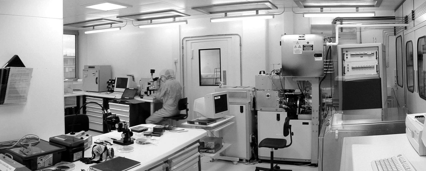
The Group is well equipped with facilities for micro-fabrication. The facilities in our Class 100 clean rooms include double sided optical lithography, high temperature ovens, deep reactive ion etching, ion implantation, evaporators and sputter coaters. In addition to possessing self-sufficiency in device/system fabrication, the Group is also well equipped for the characterisation of the optical and electronic properties of materials, devices, circuits and systems. Material characterisation is done using AFM, KFM and electrical measurements under high magnetic fields and cryogenic temperatures. Most optical characterisation is performed at the standard telecommunications wavelength of 1.5 µm. DC electrical characterisation can be performed in a temperature range of 10K - 350K, while RF characterisation can be performed up to 8.5 GHz. We have our own RF probe station and access to a new network analyser.
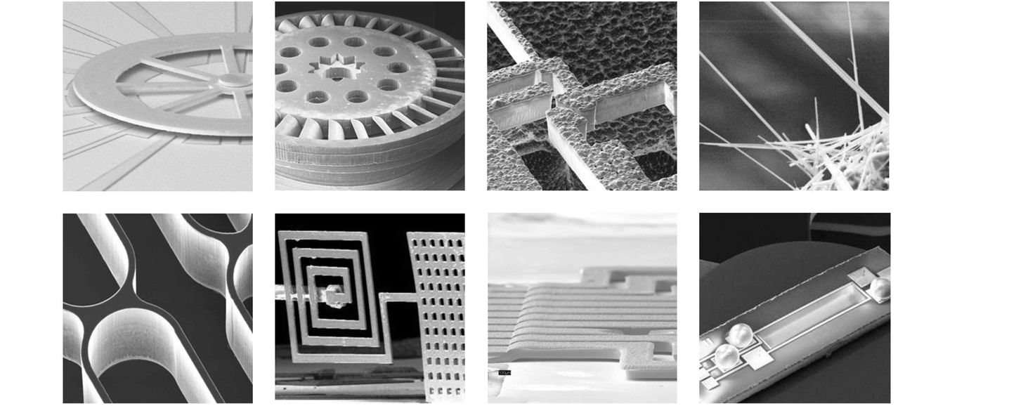
Our main topics of research currently are: 3-D microstructure fabrication, self-assembly techniques and micro-mechanical actuators; integrated optical devices on silicon for fibre communication systems; electronic heterostructure devices and circuits in SiGe alloys and SiGe on insulator (SGOI); nano-lithography and electrochromic systems for 'smart' windows. An important area of future development for the Group is the integration of sensing, actuation, optics and electronics into micro systems for providing entirely new functionality to all types of traditional 'macro' systems. We hope that our unique approach and combination of skills will allow us to make innovative contributions in this developing field.
Head of Group, Deputy Head of Group
Professor Andrew Holmes
Professor Andrew Holmes
Head of Group
Dr Zahid Durrani
Dr Zahid Durrani
Deputy Head of Group
Apply for a PhD
The OSD Group is always looking for talented PhD candidates.
To learn more about the application process for postgraduate research, including entry requirements, selection criteria, and financial support, please read the departmental guidance on applying to study for a PhD.

