Integrated magneto-optic Micro traps in atom chips
Atom chips combine cold atom physics with microfabrication techniques to create and manipulate electric, magnetic and optical fields to trap and manipulate atom clouds. In prototype devices, atom chips are already being used to make Bose Einstein condensates and also for applications including clocks, atom interferometry, and quantum information processing.
In experiments to date, atoms are typically initially collected from a warm vapour by a magneto-optical trap (MOT), which holds them as a mm-sized cloud at microKelvin temperatures . The atoms then have to be transferred from the macroscopic MOT cloud to the microscopic traps in the chip. With this loading method, alignment of the traps can be tedious and the atoms are not easily distributed over many micro-traps. We are developing a new approach in which microscopic MOTs integrated into the chip collect small atom clouds in the same location in which they can later be transferred to tighter traps for further manipulation.
The Experiment
This experiment uses the principle of the pyramid Magneto-Optical Trap which requires only a single circularly polarized laser beam to trap atoms . [1]
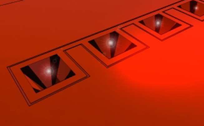
A Si wafer cut on the {100} plane is coated with silicon nitride in which square openings are then made by dry etching. This forms a mask for anisotropic etching in KOH, which reveals the {111} planes, making hollow pyramids in the surface of the silicon. The crystal structure in silicon dictates that the angle between opposite faces is 70.5° rather than 90° which is found in a standard pyramid MOT. However our experiments on a macroscopic sized version of the pyramid have already shown that the MOT can nevertheless be made to work with the 70.5° geometry.
The photo to the right illustrates a recently produced array of silicon micropyramids, fabricated using the facilities at the London Centre for Nanotechnology
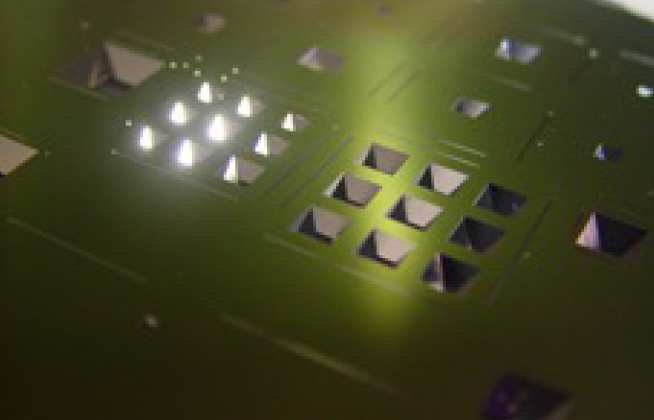
Current-carrying wires are integrated into the chip around the pyramid openings as can be seen in the picture below. These, combined with a uniform bias field provide the quadrupole magnetic field profile required to complete the MOT.
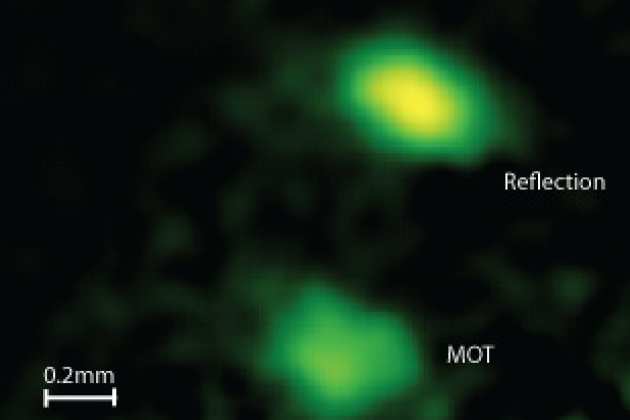 We have successfully demonstrated trapped atoms inside silicon microfabricated pyramids on the 4mm scale. The image on the right is a false colour image of approximately 3000 atoms trapped inside one of these pyramids. The MOT is less bright than its reflection as the image of the MOT is positioned above a region of bright scatter inside the pyramid impairing the imaging process.
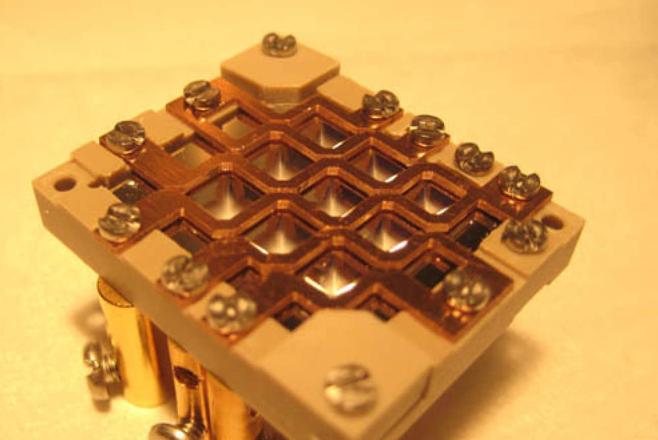
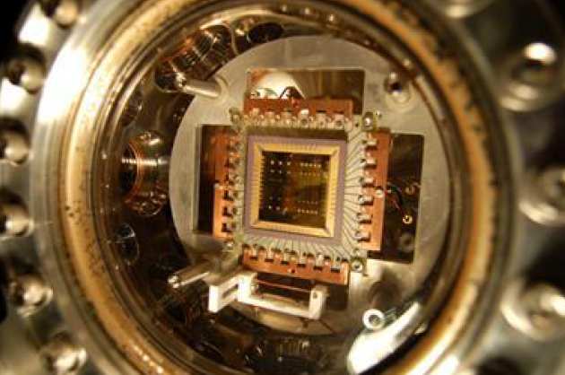
The image below shows an integrated device manufacture in conjunction with our collaborators at Southampton University showing pyramids ranging from 1.2mm to 200 microns in diameter inside our vacuum chamber. The silicon wafer is mounted in an industry standard CGPA (Ceramic Pin Grid Array) and the whole package is inserted into a FR4 circuit board creating a fully UHV compatible assembly.
For more details contact Joe Cotter (j.cotter [at] imperial [dot] ac.uk).
Characteristics of integrated magneto-optical traps for atom chips
S. Pollock, J. P. Cotter, A. Laliotis, F. Ramirez-Martinez and E. A. Hinds
New Journal of Physics 13, 043029 (2011) (Selected as a journal highlight for 2011)
Integrated magneto-optical traps on a chip
S. Pollock, J. P. Cotter, A. Laliotis, E. A. Hinds
Optics Express Vol. 17, Iss. 16, pp. 14109–14114 (2009)
Fabrication of Magneto-Optical Atom Traps on a Chip
G. Lewis, Z. Moktadir, C. Gollasch, M. Kraft, S. Pollock, F. Ramirez-Martinez, J. P. Ashmore, A. Laliotis, M. Trupke, E. A. Hinds
IEEE Journal of Micro-Electro-Mechanical Systems, 18 (2). 347 -353 .(2009)
Pyramidal micromirrors for microsystems and atom chips
M. Trupke, F. Ramirez-Martinez, E. A. Curtis, J. P. Ashmore, S. Eriksson, E. A. Hinds, Z. Moktadir, C.Gollasch, M. Kraft, G. Vijaya Prakash, and J. J. Baumberg.
Applied Physics Letters, 88, 2006.