A high degree of control in the manipulation of quantum states can today be achieved by means of small-scale, integrated devices known as atom chips. These offer the advantage of miniaturisation and precise and flexible control of ultra-cold atoms, for potential applications in quantum information and in the study of low-dimensional quantum gases. Both these applications require the ability to detect and manipulate low atom numbers. For this purpose, one of our aims is to integrate microscopic optical components on our atom chips.
In our permanent-magnet atom chip (Fig. 1), a pattern of magnetisation recorded in commercial videotape generates the appropriate magnetic field to allow the confinement of cold atoms at distances less than 100 micrometres from the chip surface. Our chip offers the possibility of trapping ultra-cold 87Rb atoms in arrays of 1-6 very elongated high-aspect-ratio traps (Fig.2, 3, 4) where tight transverse confinement brings the system close to the one-dimensional (1D) quantum gas regime.
Permanent Magnet Atom Chips - BEC on a videotape
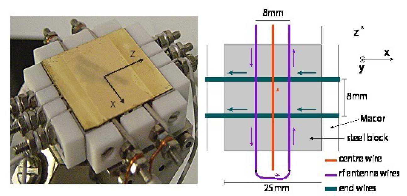
Fig. 1. photograph of the videotape atom chip. Right: schematic view of the wires under the chip. The arrows indicate the direction of the currents in the wires.
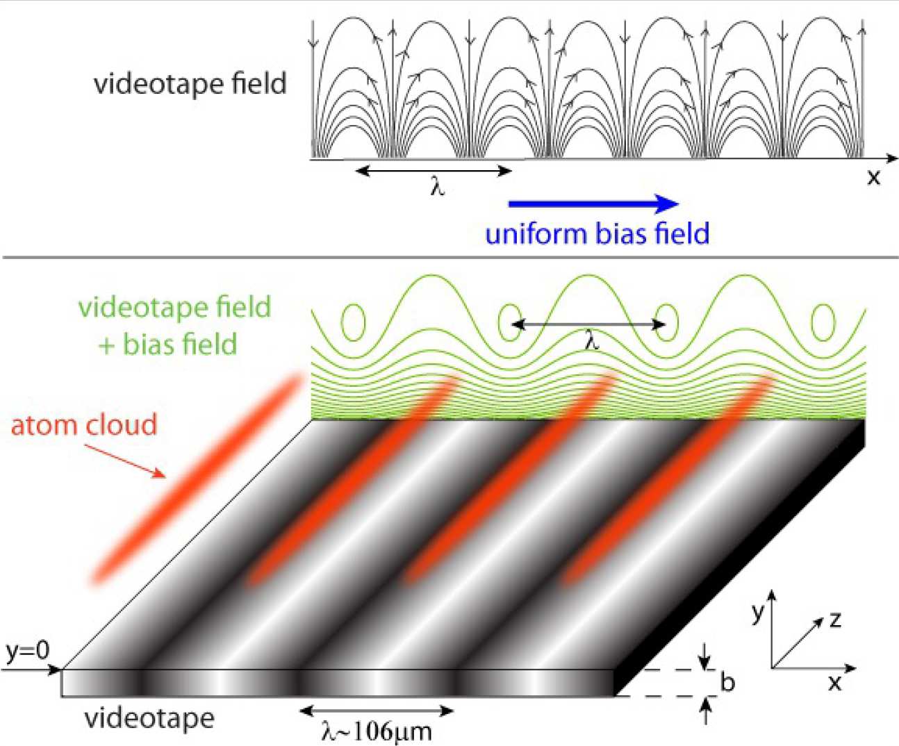
Fig. 2. Magnetic fields used to create an array of videotape magnetic micro-traps. Top: field lines generated by the sinusoidally magnetised videotape, and uniform bias field. Bottom: contours of constant magnetic field strength of combined videotape field and bias field. As a result, atoms can be trapped in an array of elongated magnetic traps separated by a distance µ~106µm along x.
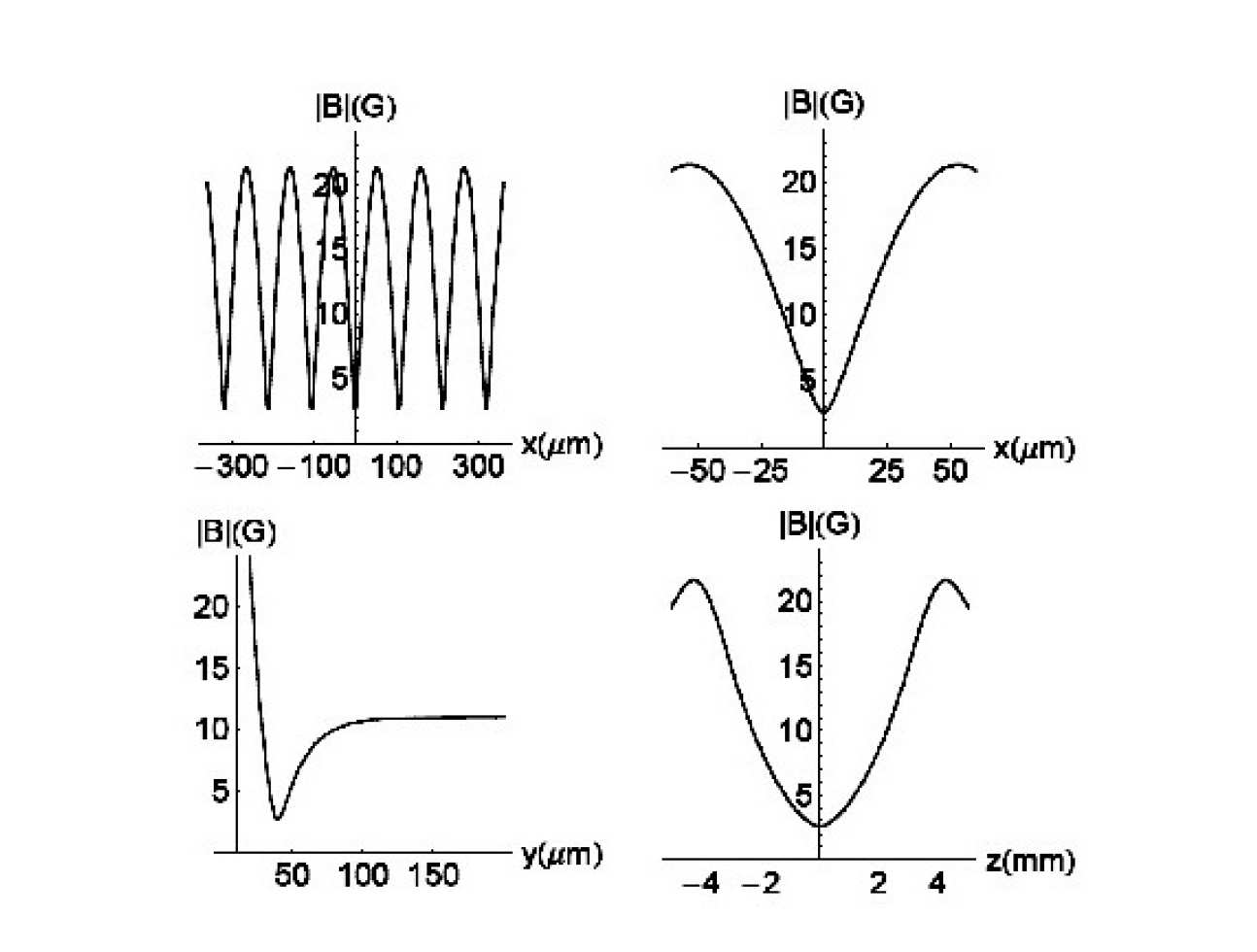
Fig. 3. Total magnetic field strength in the videotape magnetic traps as a function of the x, y and z coordinates. The trap is at a distance of 40µm from the chip surface.
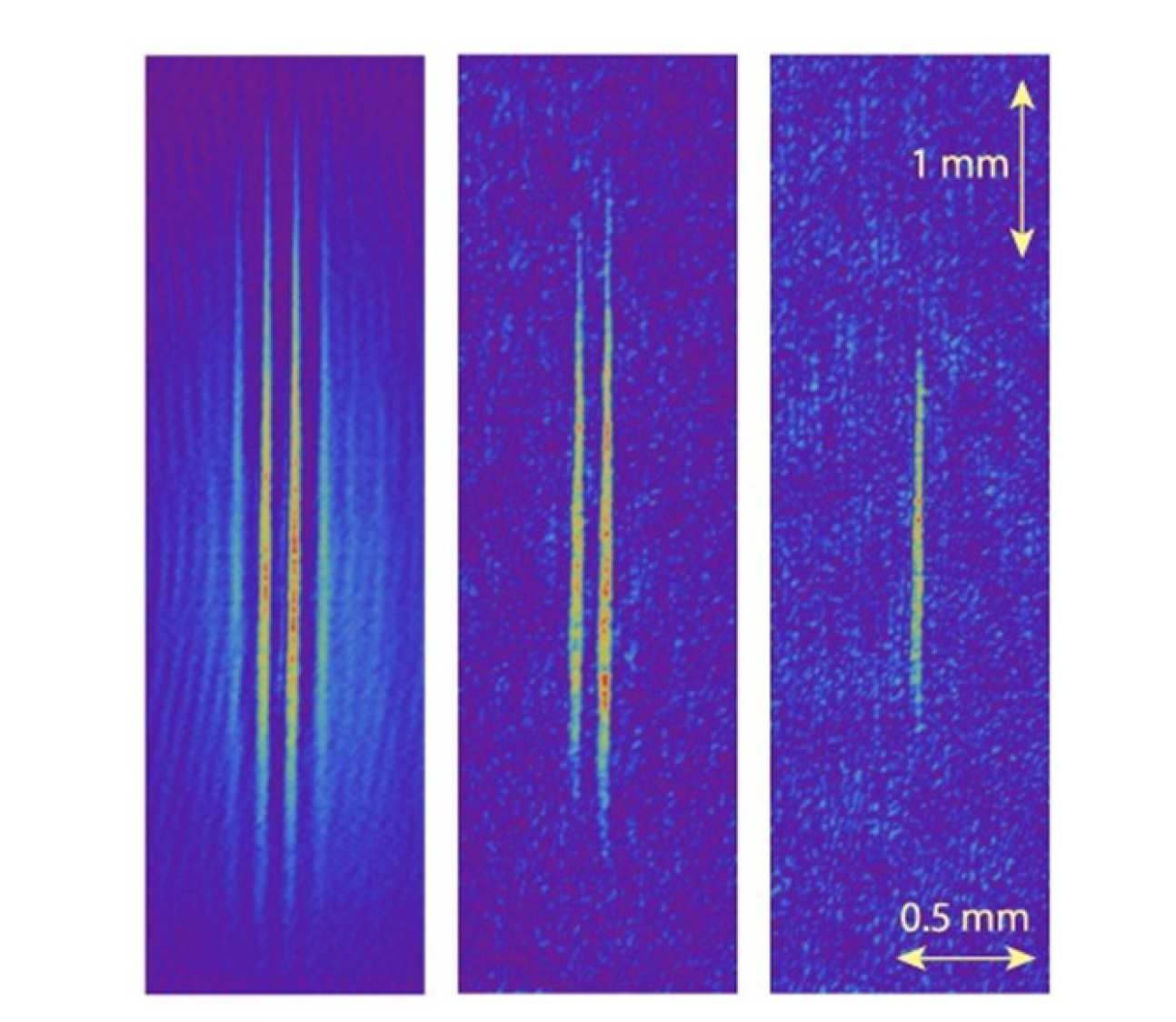
Fig. 4. In-trap absorption images of atoms loaded into one or several videotape traps. From left to right, the temperature of the best-loaded (central) videotape trap decreases from 50µK to 10µK. The length scale is the same for all images.
Permanent Magnet Atom Chips - BEC on a videotape
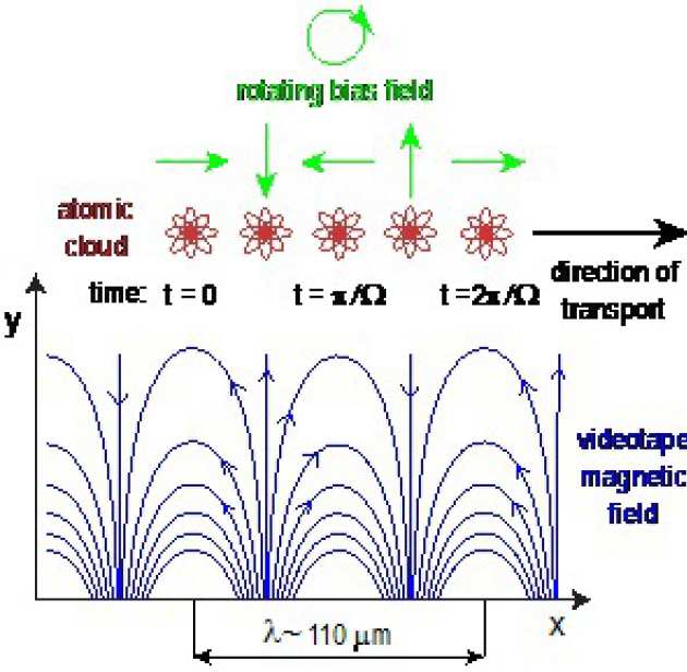
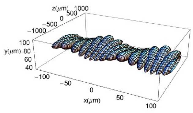
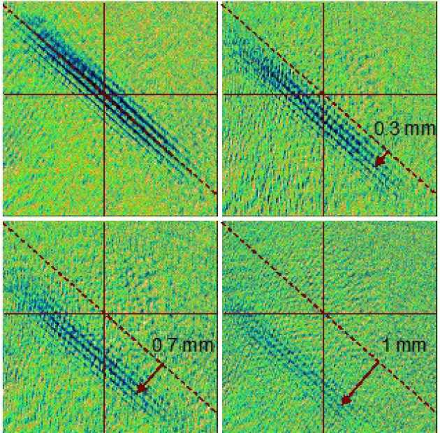
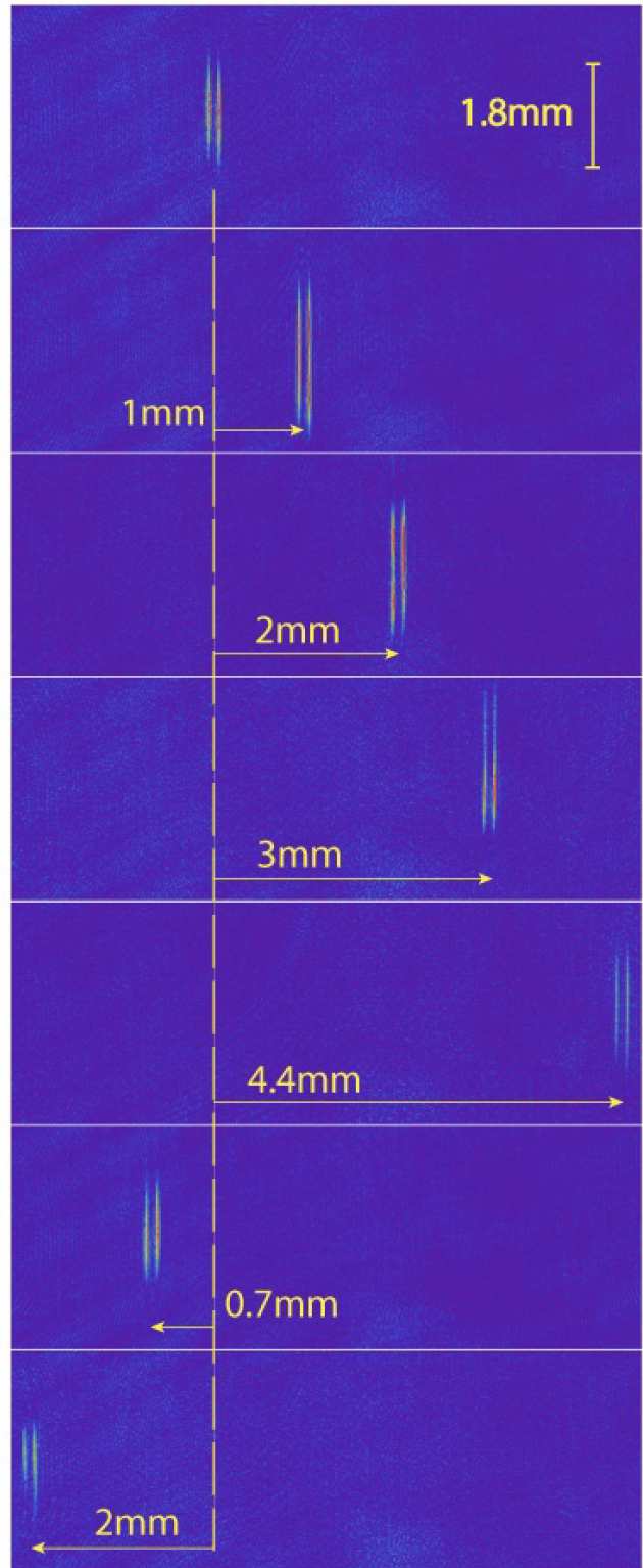
One of our main results is the implementation of the transport (Fig. 1, 2) of these arrays of elongated atom clouds parallel to the surface of the videotape chip over distances larger than 7mm (Fig. 3, 4). This can be used to convey the confined atoms from an initial trapping region into a detection region in a very precise and controlled way.
|
Fig. 1. Idea of the transport mechanism used to displace the trapping potential along x. The videotape magnetic field lines are shown in blue and the rotating bias field in green. As the orientation of the bias field changes in time during one rotation, the traps translate along x by a distance equal to λ. The bias-field rotation frequency is Ω/(2π). |
|
Fig. 2. Plot of the calculated constant potential energy contour (230µK) during two full transport cycles, as a trap moves from x = -110µm to x = 110µm. Each contour corresponds to a different time during transport and gravity is included in the calculation. |
|
Fig. 3. Absorption images of an array of 5-6 videotape magnetic traps transported parallel to the chip surface, along the x direction. Clockwise from the top left, the transported distances are: 0, 0.3mm, 0.7mm and 1mm, corresponding to 0, 3, 6 and 9 cycles of bias field rotation at a frequency of 50Hz. The solid and dashed lines are fixed at the same position on all images. |
|
Fig. 4. Sequences of absorption images of cold atoms (16µK) confined in two videotape traps and transported along the transverse direction of the traps over the indicated distances, to either side of their initial loading position. The frequency of bias field rotation is 50Hz, and the trap height is 68µm. |
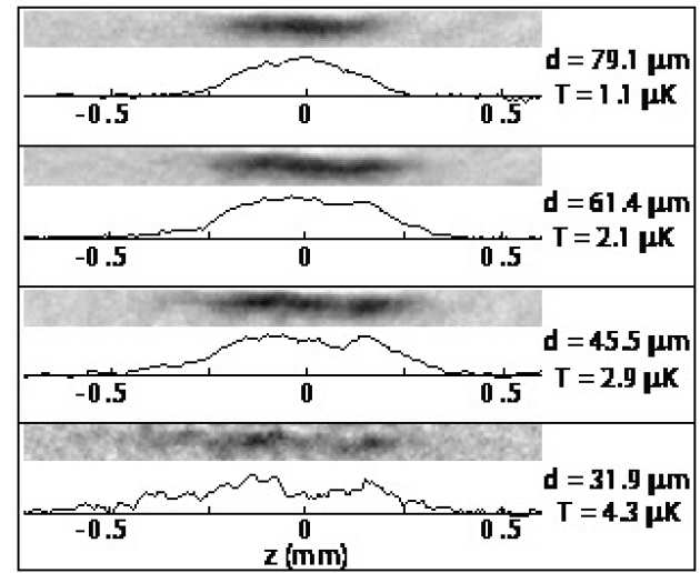
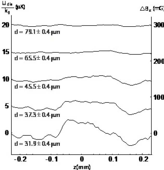
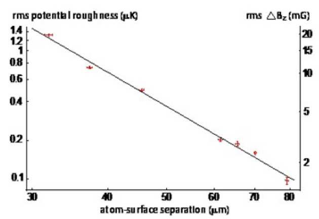
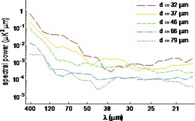
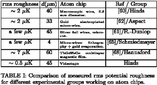
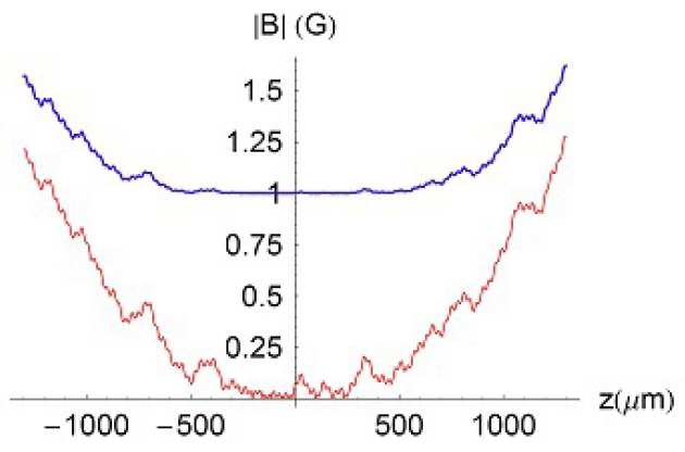
We have also studied the effect of the roughness of the videotape trapping potential on the shape of the trapped cloud. Cold atomic clouds show a smooth density distribution when trapped at distances larger than 100 micrometres from the chip surface. For shorter distances to the chip, the clouds break up in fragments (Fig. 1) revealing the roughness of the trapping potential (Fig. 2, 3, 4). We believe this roughness results from defects in the videotape. We have recently characterised in detail the strength of these fragmentation effect at several distances from the chip surface and found a scaling law for the amplitude of the corrugated potential as a function of atom-surface distance. We have also developed theoretically a powerful way to control and suppress these fragmentation effects by combining the DC fields that form our present videotape atom traps with AC oscillating fields (Fig 5).
|
Fig. 1. Fragmentation in a videotape atom trap at different distances, d, from the chip surface. The absorption images and axial linear density profiles show how the corrugations in the trapping potential are more pronounced for small atom-surface separations. |
|
Fig. 2. Axial disorder potentials (Udis) measured with ultra-cold atoms in videotape magnetic traps. Each curve corresponds to a different atom-surface separation, d, that decreases from top to bottom, as indicated by the labels, and is an average of 4-6 experimental realisations. The potentials have been offset vertically from each other by 5K for clarity. The anomalous axial magnetic field, Bz, is also shown. |
|
Fig. 3. Rms potential roughness and rms amplitude of the axial magnetic field corrugations as a function of atom-surface separation, d, (logarithmic scales). The data points are obtained from measurements with cold atoms confined in videotape traps. Each data point results from the analysis of 4-6 absorption images coming from different realisations of the experimental sequence. The solid line shows a linear fit of the data that yields a dependence of roughness on atom-surface separation of d-2.7. |
|
Fig. 4. Fourier power spectra of the disorder potentials measured in the videotape traps for different atom-surface separations, d. |
|
|
|
Fig. 5. Predicted reduction of the axial potential roughness by cancelling the net axial offset field and superimposing a rotating transverse field of amplitude 1G. The thin red line shows the static magnetic field strength with disorder, including the end-wire field, before the rotating field is added. The thicker blue line shows the time-averaged field strength after adding the rotating field. The trapping potential is proportional to the magnetic field strength. |
As for the integration of microscopic optical components on atom chips, the videotape atom chip has now been replaced by a new chip that contains optical waveguides (see Optical Waveguide Chip section) which will allow studies of interaction of light with atoms and highly sensitive atom detection.
The combination of all these techniques, ie., the possibility of trapping the atoms in very elongated traps, the implementation of the controlled transport of cold atom clouds over large distances and the integration of optical waveguides onto our chips, will open up the possibility of studying one-dimensional quantum gases and realising a 1D superfluid to Mott insulator transition, as well as providing the first step towards a quantum register for a string of atomic qubits, with a view to performing quantum information experiments.
Cold atoms in videotape microtraps C. D. J. Sinclair, J. A. Retter, E. A. Curtis, B. V. Hall, , I. Llorente-Garcia, S. Eriksson, B. E. Sauer and E. A. Hinds, Eur. Phys. J. D. 35, 105-110 (2005).
Bose-Einstein condensation on a permanent-magnet atom chip C. D. J. Sinclair, E. A. Curtis, I. Llorente-Garcia, J. A. Retter, B. V. Hall, S. Eriksson, B. E. Sauer and E. A. Hinds, PRA 72, rapid communication (2005)
Permanent-magnet atom chips for the study of long, thin atom clouds I. Llorente-Garcia, C. D. J. Sinclair, E. A. Curtis, S. Eriksson, B. E. Sauer and E. A. Hinds, Journal of Physics: Conference Series (Cold Atoms and Molecules near Surfaces) 19, 70-73 (2005).
Preparation of a Bose-Einstein condensate on a permanent-magnet atom chip C. D. J. Sinclair, E. A. Curtis, J. A. Retter, B. V. Hall, , I. Llorente-Garcia, S. Eriksson, B. E. Sauer and E. A. Hinds, Journal of Physics: Conference Series (Cold Atoms and Molecules near Surfaces) 19, 74-77 (2005).
