Our state-of-the-art multidisciplinary facilities offer researchers and students a highly collaborative and well supported environment for learning and conducting innovative, world-leading research
The Department of Bioengineering provides world-class facilities for micro- and nanofabrication, supporting the development of advanced technologies at the micro- and nano-scale. These interdisciplinary laboratories are specifically equipped for research in areas such as lab-on-a-chip and organ-on-a-chip systems, among other emerging applications.
The facilities are managed by a highly experienced, PhD-level technical staff, ensuring efficient and reliable delivery of key technologies. This dedicated support also facilitates the retention and transfer of specialised technical knowledge, which is critical to maintaining the department’s leadership in international research and innovation.
Access to these facilities is available to all members of the department, as well as researchers from the broader Imperial College community and external collaborators.
Micro and Nanofabrication Facilities
CRUK Microfabrication Facility
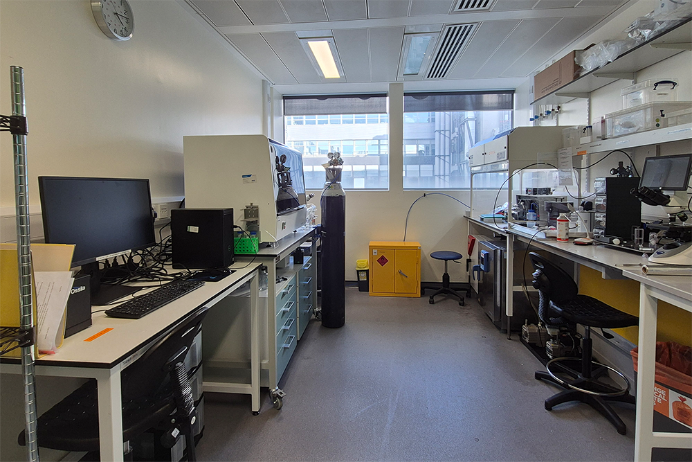

This facility offers a full range of services for prototyping SU-8 and PDMS micro-devices, including a clean lab. The user-friendly setup of the facility enables researchers from different disciplines to perform SU-8 photolithography and PDMS micro-chip casting with a high resolution of 5 µm and a broad thickness range from 5 µm to 250 µm. The training process is quick, and you can use the facility after 2 days of training.
For more information about training and access to the facility, please check the "New User" page on Wiki.
Bionanofabrication Clean Room Core Facility
 The Bionanofabrication Clean Room Core Facility at the White City campus offers various equipment and processes to bring microfabrication technologies to biology and biomedical applications. This platform is based on level 6 of the Sir Michael Uren Hub in the bioengineering technology platform hub.
The main equipment available are: an ALD, ICP Deposition and ICP etching Plasma cluster from Oxford Instruments.
This laboratory has been designed with the desire to allow researchers of various fields to develop innovative ideas using state of the art microfabrication equipment and technology in a safe controlled environment. The laboratory is used by researchers across Imperial College to develop high resolution microfluidics projects, medical nanodevices, nanosensors and cell interfacing devices.
See below for more details.
Imaging essential information, access, contacts
CRUK Microfabrication Core Facility - South Kensington
The CRUK Microfabrication Facility includes a yellow clean-lab optimised explicitly for the prototyping of negative photoresists, such as the SU-8 series. The facility's segregated design enables high-resolution patterning down to 5 μm and supports the fabrication of structures with a wide range of thicknesses. Here is the list of offered services.
Photolithography Yellow Laminar Hood
.png)
This station features a state-of-the-art yellow laminar flow hood designed to support high-precision spin coating and thermal processing of photoresist films for micron-scale photolithography. It is equipped with the following instruments:
- Hotplate EMS 1000-3
- Spin Coater WS-650MZ Modular
- Hotplate Torrey Pines
These components collectively enable:
- Photolithographic fabrication with a resolution down to 5 µm
- Uniform coating of various substrates, including 3-inch and 4-inch wafers, as well as standard glass slides
- Validated protocols for producing SU-8 photoresist layers across a broad range of thicknesses
- Programmable thermal processing, allowing precise control of temperature gradients and automation of extended baking steps for photoresist curing
Masked and Maskless Exposure
The facility offers masked and maskless UV exposure with a user-friendly state-of-the-art UV-KUB mask aligner and Smart-Print UV maskless system.
UV-KUB 3 Mask Aligner
.png)
The UV-KUB 3 is a new generation of compact mask aligner which can provide:
- Resolution of 1 µm
- The alignment accuracy of 1 µm
- Complex (physical) or soft (proximity) contact processes
- 100 numbers of programmable cycles
Smart Print UV
.png)
The Smart Print UV is a versatile, maskless photolithography tool that utilises advanced UV light engine technology. It is designed for high-resolution, direct-write patterning and offers a range of capabilities, including:
- Two-dimensional patterning with a line resolution as satisfactory as 1.5 µm
- Ability to fabricate complex geometries without the need for physical masks
- Compatibility with a broad range of SU-8 photoresist thicknesses
Support for various substrate types - Multi-layer alignment functionality for sequential patterning
Intuitive, user-friendly software interface for streamlined operation
Surface Characterisation
The CRUK Microfabrication Facility provides advanced tools for high-resolution surface characterisation, including a state-of-the-art optical profilometer and an Olympus bidirectional optical microscope equipped with dark-field imaging capability.
.png)
The Filmetrics Profilm 3D optical profilometer uses state-of-the-art white light interferometry(WLI) to measure surface profiles and roughness.
- Intuitive Analysis Software
- All 47 standard ASME/EUR/ISO roughness parameters
- Multiple Step-height techniques: line, rectangle, and histogram
- Roughness and waviness cutoff filter
- Bearing ratio
- Spatial and FFT filtering
- Volume calculation
- Form removal
The CRUK Microfabrication Facility features a dedicated white clean-lab optimised explicitly for prototyping microfluidic and lab-on-chip devices. The facility’s controlled environment supports users at various experience levels, including undergraduate students and advanced researchers, enabling them to design, fabricate, and test microfluidic systems efficiently.
The following services are offered within the white clean-lab:
Microfluids Test Bench
.png)
This setup provides a versatile microfluidics testing platform, suitable for applications ranging from entry-level instructional tutorials to the advanced evaluation of functional prototypes.
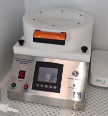
PDMS Casting and Coating
.png)
This station is specifically designed to support PDMS casting and coating within a controlled environment, ensuring both ease of use and reproducibility. A validated protocol is provided as a step-by-step recipe sheet, enabling even inexperienced users to perform the procedures independently and confidently.
Plasma Treatment
.png)
This station is equipped with a Harrick Plasma Cleaner, which is used to perform oxygen or air plasma treatments on various samples. Common applications include bonding of PDMS to glass, surface treatment of silicon wafers, and plasma cleaning of materials. To ensure both safety and ease of use, the facility provides a detailed, step-by-step Standard Operating Procedure (SOP) for operating the plasma cleaner.
BioDot Omnia Dispenser
.png)
The BioDot Omnia™ is a high-precision, low-volume dispensing system designed for applications where the size and spatial placement of liquid droplets are critical. This platform delivers picoliter-, nanoliter-, and microliter-scale droplets with exceptional accuracy and speed, leveraging BioDot’s proprietary Rainmaker™ and BioJet™ technologies.
Key Features:
- Dual dispensing capabilities: Aspirate/Dispense and Direct Dispense
- Motorised movement across X, Y, and Z axes for precise positioning
- Dispensing area of 365 × 250 mm
- Compatibility with a variety of substrates, including slides, microplates, and membranes
- Integrated wash and vacuum stations to maintain dispensing integrity
- Vision LITE camera system for real-time alignment and positioning
- ILD5000 In-Line Degasser to ensure bubble-free fluid delivery
- Controlled via a PC workstation equipped with LINK2020 software
- Supports both research and development (R&D) as well as production-scale throughput
- User-friendly software interface for streamlined operation
- Horizontal and vertical cameras for multi-angle visualisation
- Ultrasonic wash station for enhanced cleaning efficiency
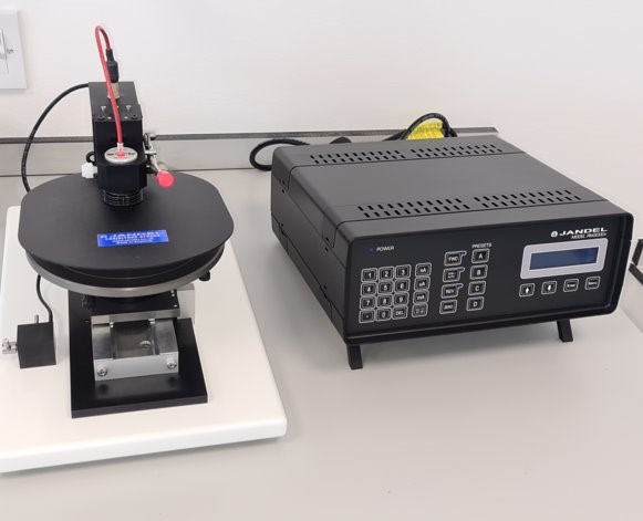
Contact angle giometer
.png)
The Ossila Contact Angle Goniometer is a user-friendly instrument designed for the precise measurement of surface contact angles and the surface tension of liquid droplets
CRUK Microfabrication Facility
The CRUK Microfabrication Facility welcomes researchers from both academic institutions and industry, including R&D scientists from commercial organisations.
To request training, gain access, or arrange a tour of the facility, please contact the Facility Managers, Dr. Shahrzad Forouzanfar and Dr. Florent Seichepine, at s.forouzanfar@imperial.ac.uk and f.seichepine@imperial.ac.uk. They will provide guidance on the appropriate next steps.
Dr Shahrzad Forouzanfar
Assistant Microfabrication Facility Manager
Email: s.forouzanfar@imperial.ac.uk
Phone: +44 7923 242 043
Work Location: B200, 2nd floor, Bessemer Building, South Kensington Campus
Dr Florent Seichepine
Engineering Core Facilities Manager, Department of Bioengineering
Email: f.seichepine@imperial.ac.uk
Phone: +44 7395 248 415
Work Location: U619, 6th Floor, Sir Michael Uren Hub, White City Campus
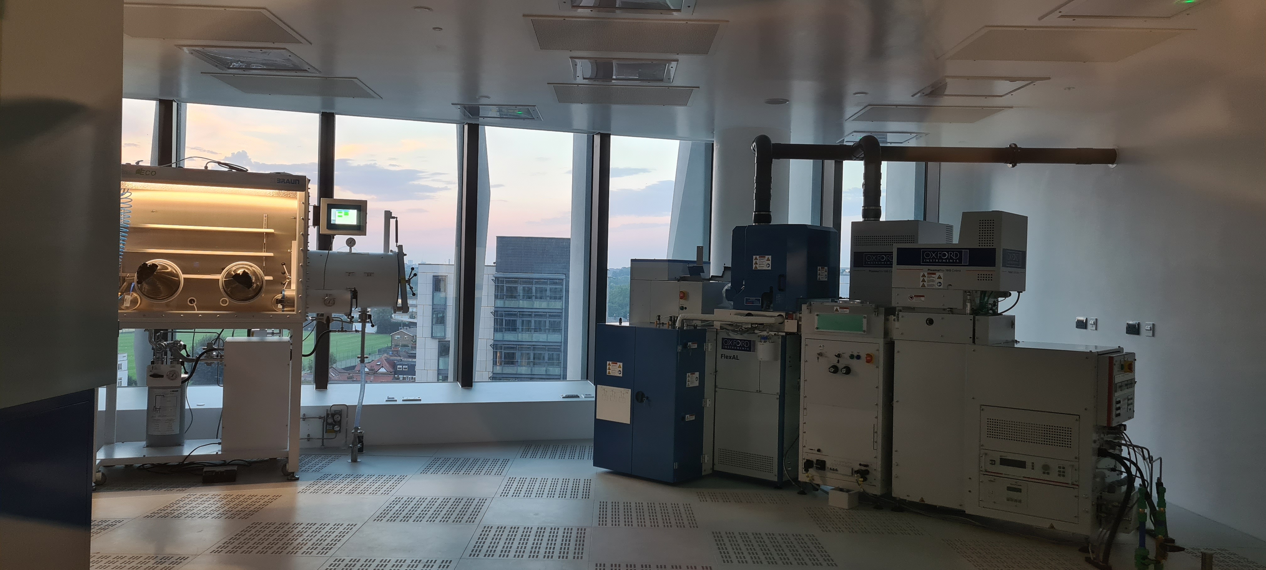
Bionanofabrication Clean Room Core Facility - White City
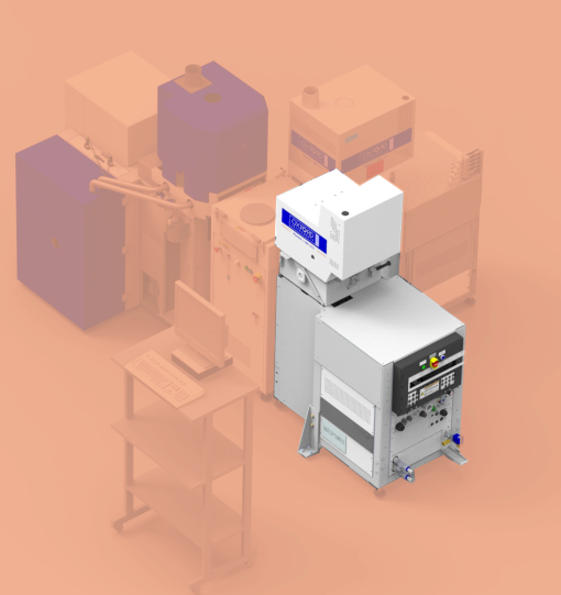
 The Oxford Instruments Plasma Cluster is composed of three chambers and a handling unit. Two PlasmaPro 100 Cobra chambers are set up as ICP deposition and ICP etching and on Flexal ALD system. Wafers can be carried from one chamber to another without exposing to air via the central handling unit.
Chamber 1: Flexal II ALD System
 The Flexal II ALD chamber is dedicated to plasma and thermal ALD deposition.
This unit is equipped with a manifold that can host up to 3 precursors as well as water vapor and hydrogen gas.
This chamber allows for the deposition of extremely conformal film with an atomic precision.
Current materials available include: Al2O3, TiO2, TiN and HfO.
Chamber 2: PlasmaPro 100 Cobra ICP Etching
The ICP Etching chamber has been designed to offer versatile etching capabilities adapted for the fabrication of complex structures in silicon and other materials. The local gaspod offers the possibility of fast switching Bosch process for high aspect ratio structures. The system is equipped for silicon etching, glass etching, chlorine etching, teflon deposition and more.
Chamber 3: PlasmaPro 100 Cobra ICP Deposition
 The ICP deposition chamber allows for fast deposition of thick layer of silicon oxide and silicon nitride using silane precursors. It also allows for controlled process monitoring using in-situ spectrometric reading.
Etching and chemical treatment hood
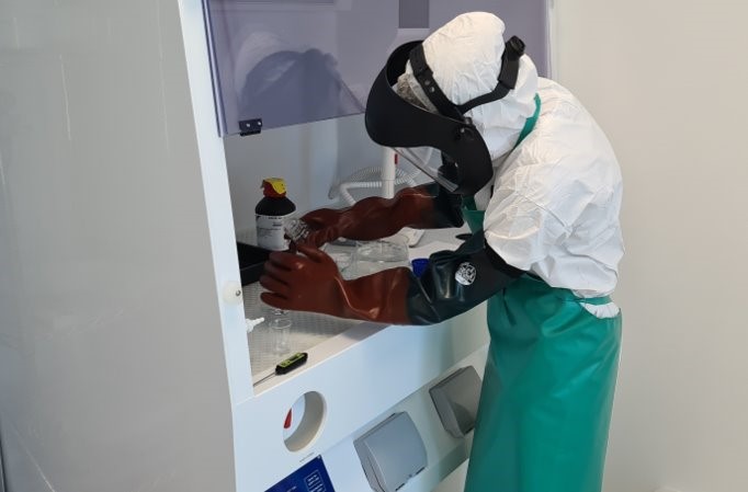
This downflow cabinet and adapted safety procedure allows for researchers to conduct procedures with possible safety risks in a safe and controlled environment. Etching, cleaning and electroless deposition procedure can be conducted here.
Glove box
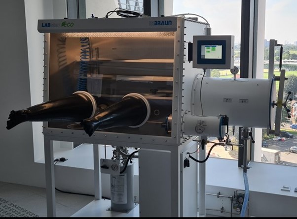
The Mbraun glove box allows for manipulation and conditioning of chemicals without any moisture or oxygen. ALD precursors can be stored and manipulated safely.
Fume hood
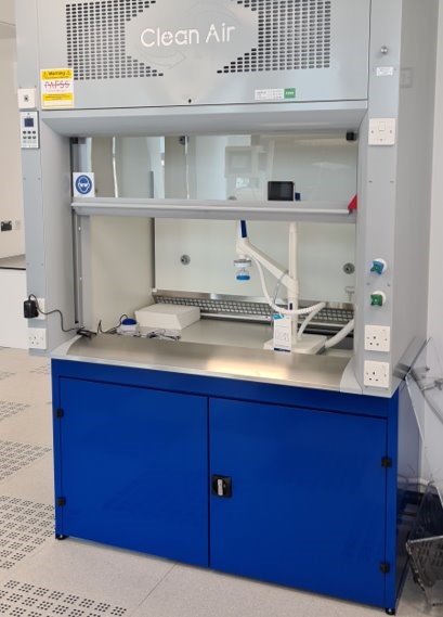
This ducted fume hood allows for various wet bench activities, solvent based processes, microfluidic system fabrication and handling of nanoparticles.
Spin coater
This spin coater from EMS is usable for various thin film fabrication from PDMS membrane to surface coating or self-assemble monolayer fabrication.
4-probe measurement system
This system is dedicated to 4-probes measurement of thin film and adapted for the fast characterisation of conductive thin film deposition or etching process.
Diener Plasma Atto
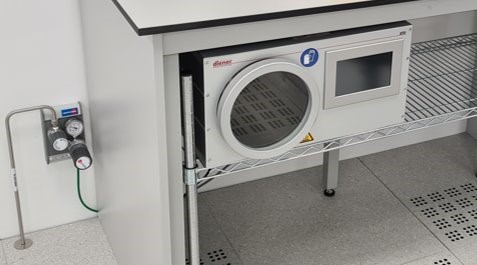
This Oxygen plasma system is dedicated to the surface cleaning and preparation of sample surfaces.
Engineering contacts
- This laboratory is dedicated to microfabrication and nanofabrication processes for life sciences and other hybrid fields. It offers a unique environment to develop niche and innovative projects in a clean and safe environment.
- It is important to note that as this laboratory presents lot of high risk processes and substances (gases, acids ...) it will not be suitable for a certain number of projects.
- Microfabrication for microfluidics should be done in the CRUK laboratory in SK when possible. Simple PDMS fabrication and oxygen treatment for Uren based experiments is possible.
- Microelectronics can be done in the Royce Institute laboratory or the CBIT clean room.
- CMOS compatible process can be done in the LCN clean room.
For Imperial users, to use the space please follow the following steps: - Before starting any projects here contact, Florent Seichepine at f.seichepine@imperial.ac.uk to discuss how suitable it is for this environment.
- If you do not have one, make an account on PPMS Bioengineering
- Complete the lab induction forms and online safety courses. More information can be found on the facility's wiki page .
- You can now use the lab. You just need to book it via PPMS system (confirmation will be needed if you are registered as Novice user)
For non-Imperial users: - Access can be arranged with various degrees of autonomy depending of the project. Please contact the lab manager: Florent Seichepine at f.seichepine@imperial.ac.uk for more information.
Dr. Florent Seichepine
Email: f.seichepine@imperial.ac.uk