Tabs 1
- Magnetron Sputtering (HIPIMS)
- E-Beam Deposition System
- Wide Beam Ion Milling
- ICP-RIE
- Surface Profiler
- Thin Film Analyser
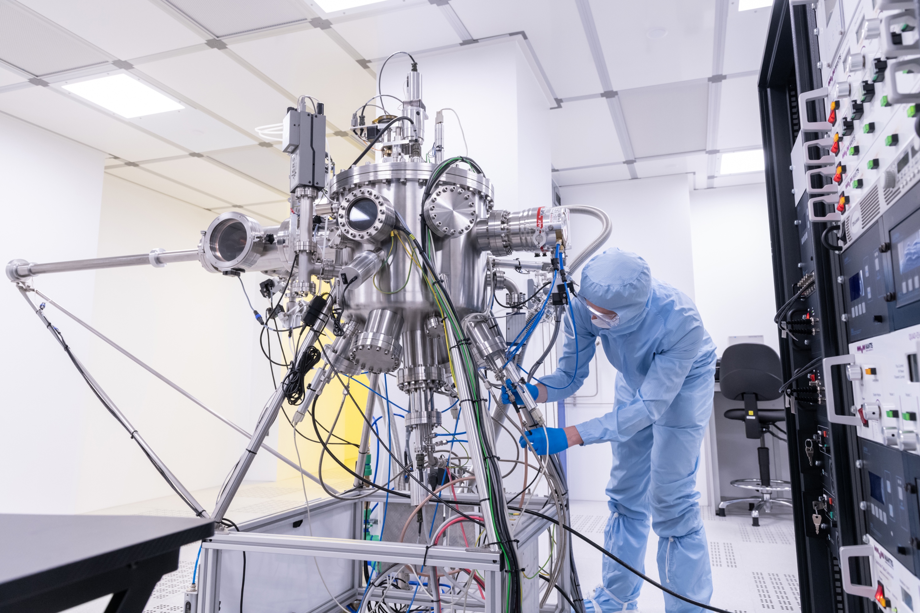 Magnetron Sputtering (HIPIMS)
The Magnetron Sputtering System is an ultra-high vacuum deposition system. It consists of three sources for DC and RF magnetron sputtering. It has a 4” in diameter rotating substrate holder with a heating stage to 800°C and RF biasing option. The system has High-Power Impulse Magnetron Sputtering (HiPIMS) deposition capability. It is equipped with two Ionautics’ HiPSTER 1 power supplies with Reactive Sputtering control and a HiPSTER synchronisation unit that allows the user to control the pulsing of both HiPSTER HiPIMS power supplies.
 The E-beam evaporation system is an ultra-high vacuum deposition system. It consists of an MBE-Komponenten Multi Pocket Electron Beam Evaporator with 4 pockets, a hearth capacity 8 cm³ each, and a maximum power of 5kW. It has a 4” in diameter rotating substrate holder with a heating stage of 800°C and QCM to monitor the thin film growth and thickness.
It is used for the precise deposition of metal thin films.
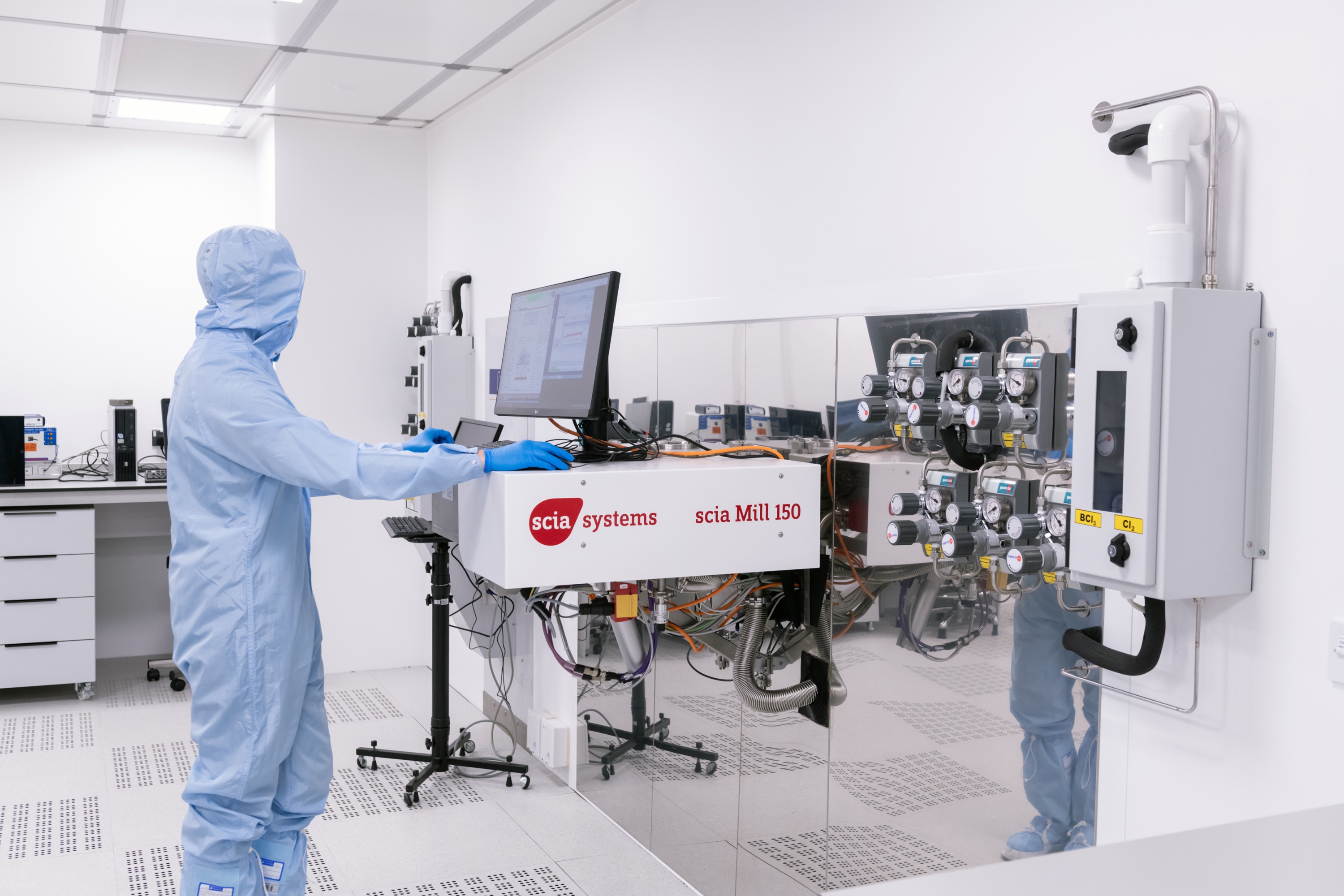 The scia Mill 150 is designed for highly uniform ion beam etching of single substrates up to 150 mm. The system is equipped with a circular broad beam ion source with a diameter of 218 mm. The source operates with inert gases (Ion Beam Etching) as well as with reactive gases (Reactive or Chemically Assisted Ion Beam Etching). The substrates will be mounted on a tiltable and rotatable substrate holder, which enables helium backside thermal contact for effective substrate cooling.
For faster processing and with stable process conditions a load lock system is installed, and samples of up to 150 mm in diameter are transferred automatically via the load lock into the process chamber.
A typical application is the nano- and micro structuring of complex multilayers of metallic and dielectric materials. An optical endpoint detection system is also integrated for the recognition of etched species and to apply a defined etch stop.
 Inductively Coupled Plasma - Reactive Ion Etching (ICP-RIE)
The PlasmaPro 100 Cobra ICP RIE system utilises a high-density inductively coupled plasma to achieve fast etch rates. The process modules offer excellent uniformity, high-throughput, high-precision, and low-damage processes for wafer sizes up to 200mm, supporting several markets, including laser optoelectronics, power electronics, RF and MEMS, and sensors.
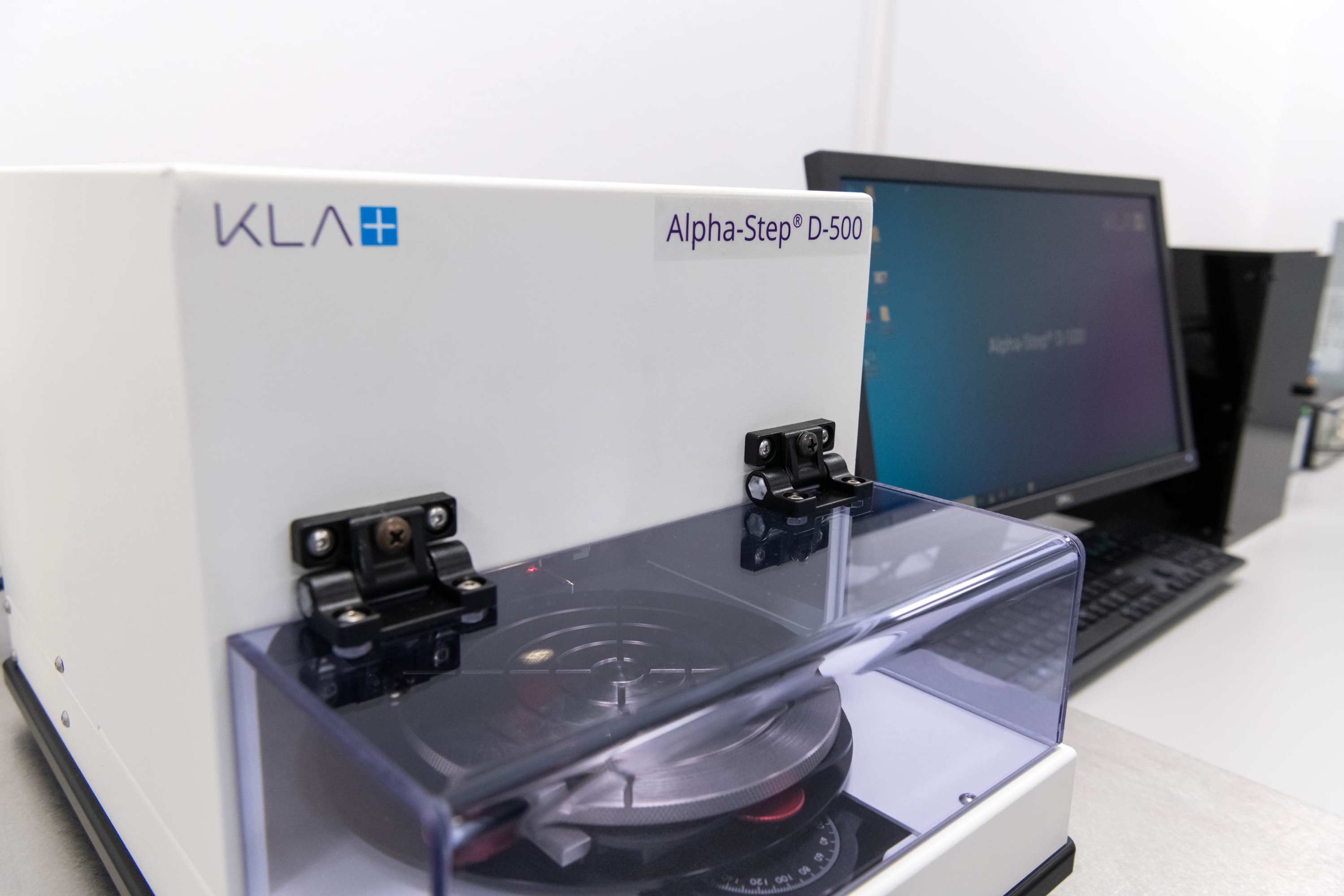 The Alpha-Step D-500 stylus profiler is capable of 2D step height measurement from a few nanometers up to 1200µm. The D-500 also supports 2D measurements of roughness, bow and stress for R&D and production environments. The D-500 stylus profilometer includes a manual 140mm stage and advanced optics with enhanced video controls.
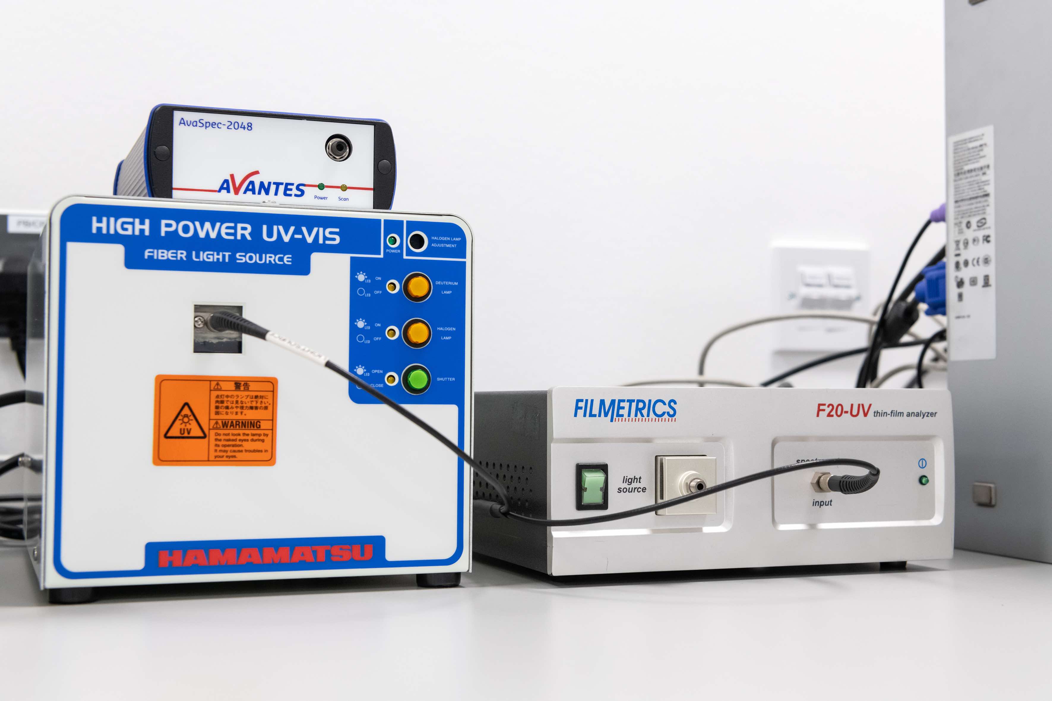 The F20–UV is a thin film analyser that can measure thickness and refractive index in less than a second. Like all thickness measurement instruments, it connects to the computer's USB port and is set up in minutes. The thickness measurement ranges between 1 nm – 40 μm, with a wavelength range between 190 – 1100 nm. Features included in the F20–UV include an integrated spectrometer, a flattening filter for highly reflective substrates, a FILmeasure standalone software for remote data analysis, reflectance standards, thickness standards, an SS-3 sample stage with fibre optic cable and a TH1-lamp.
Clean Room Yellow Room Photolithography Suite
 Easy to use and compact in size, the SUSS MicroTec MJB3 represents the perfect system for laboratories and small-volume production. As an inexpensive photolithography solution, the MJB3 has set industry standards specifically for processing small substrates and pieces up to 100 mm. Equipped with a reliable, high-precision mask alignment and high-resolution printing capability in the submicron range, the MJB3 is unsurpassed by any comparable machine.
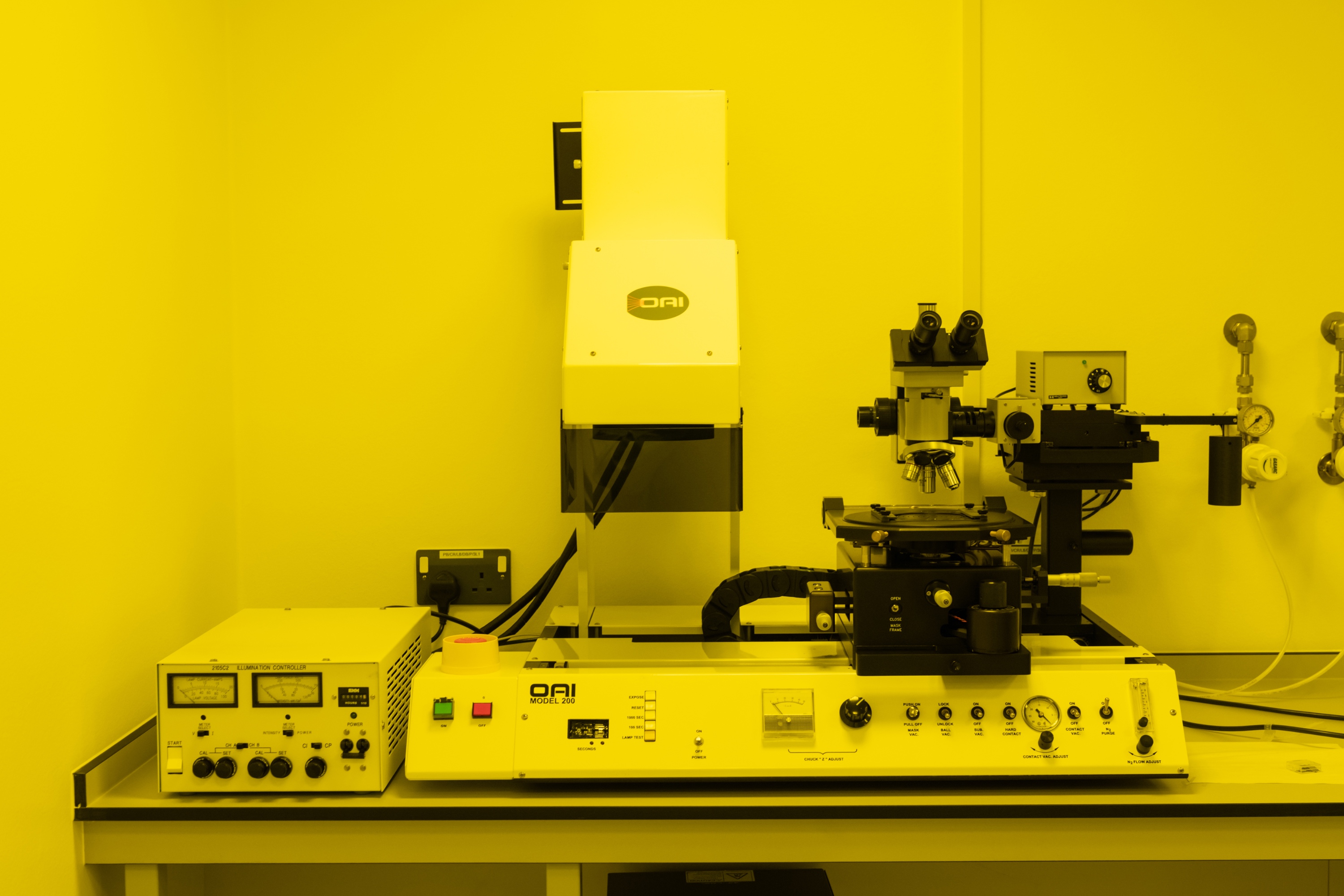 The Model 200 is a tabletop mask Aligner that requires minimal cleanroom space. It offers an economical alternative for R&D, or limited scale, pilot production. Utilising an innovative, air-bearing/vacuum chuck levelling system, the substrate is levelled quickly and gently for parallel photo mask alignment and uniform contact across the wafer during contact exposure. The system is capable of one-micron resolution and alignment precision.
The alignment module features mask insert sets and quick-change wafer chucks that facilitate using various substrates and masks without requiring special tools for reconfiguration. The alignment module incorporates micrometres for the X, Y, and Z-axis. The Model 200 Mask Aligner features a dependable OAI UV Light Source, which provides collimated UV light in Near or Deep UV using lamps ranging in power from 200 to 2000 watts.
Dual-sensor optical feedback loops are linked to the constant intensity controller to provide control of exposure intensity within ±2% of the desired intensity. This Mask Aligner is a flexible, economical solution for any entry-level mask alignment and UV exposure application and is also available with a LED Light Source.
SUSS MicroTec‘s LabSpin platform represents the next generation of manual spin coater and developer systems that have been developed specifically for laboratory and R&D. Designed for various photolithography chemicals, LabSpin systems provide uniform, precise and repeatable spin coating results on the wafer through its advanced process chamber design.
The LabSpin is available in various versions, such as a tabletop and built-in unit. Built-in platforms are designed for integration into a wet bench and a glove box or are used in the SUSS LabCluster. LabSpin6 is suitable for round substrates up to 150 mm in diameter or square substrates up to 100x100 mm. LabSpin8 is suitable for round substrates up to 200 mm in diameter or square substrates up to 150x150 mm.
With a wide range of substrate holders, even fragments and unique shapes can be processed without problems. The LabSpin platform is characterised by a compact, space-saving design and requires little clean room space.
The large variety of LabSpin options allows a very wide range of applications. Coatings can be applied manually with syringes, semi-automatically with cartridges or with up to two fully automatic dispensing systems. In addition to edge coating, edge bead removal and puddle development, further options are available.
Clean Room - E-Beam Lithography Suite
Raith E- Beam Writer
The eLINE Plus is the optimum system for a broad bandwidth of nanofabrication applications with a single multifunctional electron beam lithography (EBL) system.
The advanced lithography infrastructure of eLINE Plus supports both ultra-high-resolution electron beam lithography and large-area nanofabrication. Moreover, eLINE Plus´s multifunctionality unites the worlds of electron beam lithography, nanoengineering, ultra-high resolution, and large-area SEM imaging, including dedicated features for metrology and process control.
eLINE Plus provides the following smart building blocks and concepts:
- Advanced 30 kV TFE electron optical column technology
- Innovative and unique stitch-error-free writing strategies
- Dedicated features for automated waferscale metrology and process control
- Laser Interferometer Stage
- Multiple detector concept
- Multiport vacuum chamber
- Open and upgradable platform concept
- Raith NanoSuite: comprehensive software interface with all modules fully integrated
The eLINE Plus is designed for ultimate flexibility and versatility in the field of multi-technique in-situ nanofabrication beyond classical electron beam lithography. Fully equipped with all nanoengineering options, the tool philosophy is aligned with the workflow “fabricate, relocate, modify, measure.”
How to access
To access our facilities, please email royce@imperial.ac.uk.
.jpg)